- 您现在的位置:买卖IC网 > Sheet目录203 > AOZ8304ADI (Alpha & Omega Semiconductor Inc)TVS DIODE ARRAY LOW CAP 10DFN
�� �
�
�AOZ8304A�
�Application� Information�
�The� AOZ8304A� TVS� is� design� to� protect� four� data� lines�
�from� fast� damaging� transient� over-voltage� by� clamping�
�the� over-voltage� to� a� reference.� When� the� transient� on� a�
�protected� data� line� exceeds� the� reference� voltage,� the�
�steering� diode� is� forward� bias� and� conducts� harmful� ESD�
�transients� away� from� the� sensitive� circuitry� under�
�protection.�
�PCB� Layout� Guidelines�
�Printed� circuit� board� layout� is� the� key� to� achieving� the�
�highest� level� of� surge� immunity� on� power� and� data� lines.�
�The� location� of� the� protection� devices� on� the� PCB� is� the�
�simplest� and� most� important� design� rule� to� follow.� The�
�AOZ8304A� devices� should� be� located� as� close� as�
�possible� to� the� noise� source.� The� placement� of� the�
�AOZ8304A� devices� should� be� used� on� all� data� and�
�power� lines� that� enter� or� exit� the� PCB� at� the� I/O�
�connector.� In� most� systems,� surge� pulses� occur� on� data�
�and� power� lines� that� enter� the� PCB� through� the� I/O�
�connector.� Placing� the� AOZ8304A� devices� as� close� as�
�possible� to� the� noise� source� ensures� that� a� surge� voltage�
�will� be� clamped� before� the� pulse� can� be� coupled� into�
�adjacent� PCB� traces.� In� addition,� the� PCB� should� use� the�
�shortest� possible� traces.� A� short� trace� length� equates� to�
�low� impedance,� which� ensures� that� the� surge� energy� will�
�be� dissipated� by� the� AOZ8304A� device.� Long� signal�
�traces� will� act� as� antennas� to� receive� energy� from� fields�
�that� are� produced� by� the� ESD� pulse.� By� keeping� line�
�lengths� as� short� as� possible,� the� efficiency� of� the� line� to�
�act� as� an� antenna� for� ESD� related� fields� is� reduced.�
�Minimize� interconnecting� line� lengths� by� placing� devices�
�with� the� most� interconnect� as� close� together� as� possible.�
�The� protection� circuits� should� shunt� the� surge� voltage� to�
�either� the� reference� or� chassis� ground.� Shunting� the�
�surge� voltage� directly� to� the� IC’s� signal� ground� can� cause�
�ground� bounce.� The� clamping� performance� of� TVS�
�diodes� on� a� single� ground� PCB� can� be� improved� by�
�minimizing� the� impedance� with� relatively� short� and� wide�
�ground� traces.� The� PCB� layout� and� IC� package� parasitic�
�inductances� can� cause� significant� overshoot� to� the� TVS’s�
�TPBIASx�
�clamping� voltage.� The� inductance� of� the� PCB� can� be�
�reduced� by� using� short� trace� lengths� and� multiple� layers�
�with� separate� ground� and� power� planes.� One� effective�
�method� to� minimize� loop� problems� is� to� incorporate� a�
�ground� plane� in� the� PCB� design.� The� AOZ8304A� low�
�capacitance� TVS� is� designed� to� protect� four� high� speed�
�data� transmission� lines� from� transient� over-voltages� by�
�clamping� them� to� a� fixed� reference.� The� low� inductance�
�and� construction� minimizes� voltage� overshoot� during�
�high� current� surges.� When� the� voltage� on� the� protected�
�line� exceeds� the� reference� voltage� the� internal� steering�
�diodes� are� forward� biased,� conducting� the� transient�
�current� away� from� the� sensitive� circuitry.�
�Good� circuit� board� layout� is� critical� for� the� suppression�
�of� ESD� induced� transients.� The� following� guidelines� are�
�recommended:�
�1.� Place� the� TVS� near� the� I/O� terminals� or� connectors�
�to� restrict� transient� coupling.�
�2.� Fill� unused� portions� of� the� PCB� with� ground� plane.�
�3.� Minimize� the� path� length� between� the� TVS� and� the�
�protected� line.�
�4.� Minimize� all� conductive� loops� including� power� and�
�ground� loops.�
�5.� The� ESD� transient� return� path� to� ground� should� be�
�kept� as� short� as� possible.�
�6.� Never� run� critical� signals� near� board� edges.�
�7.� Use� ground� planes� whenever� possible.�
�8.� Avoid� running� critical� signal� traces� (clocks,� resets,�
�etc.)� near� PCB� edges.�
�9.� Separate� chassis� ground� traces� from� components�
�and� signal� traces� by� at� least� 4� mm.�
�10.� Keep� the� chassis� ground� trace� length-to-width� ratio�
�<� 5:1� to� minimize� inductance.�
�11.� Protect� all� external� connections� with� TVS� diodes.�
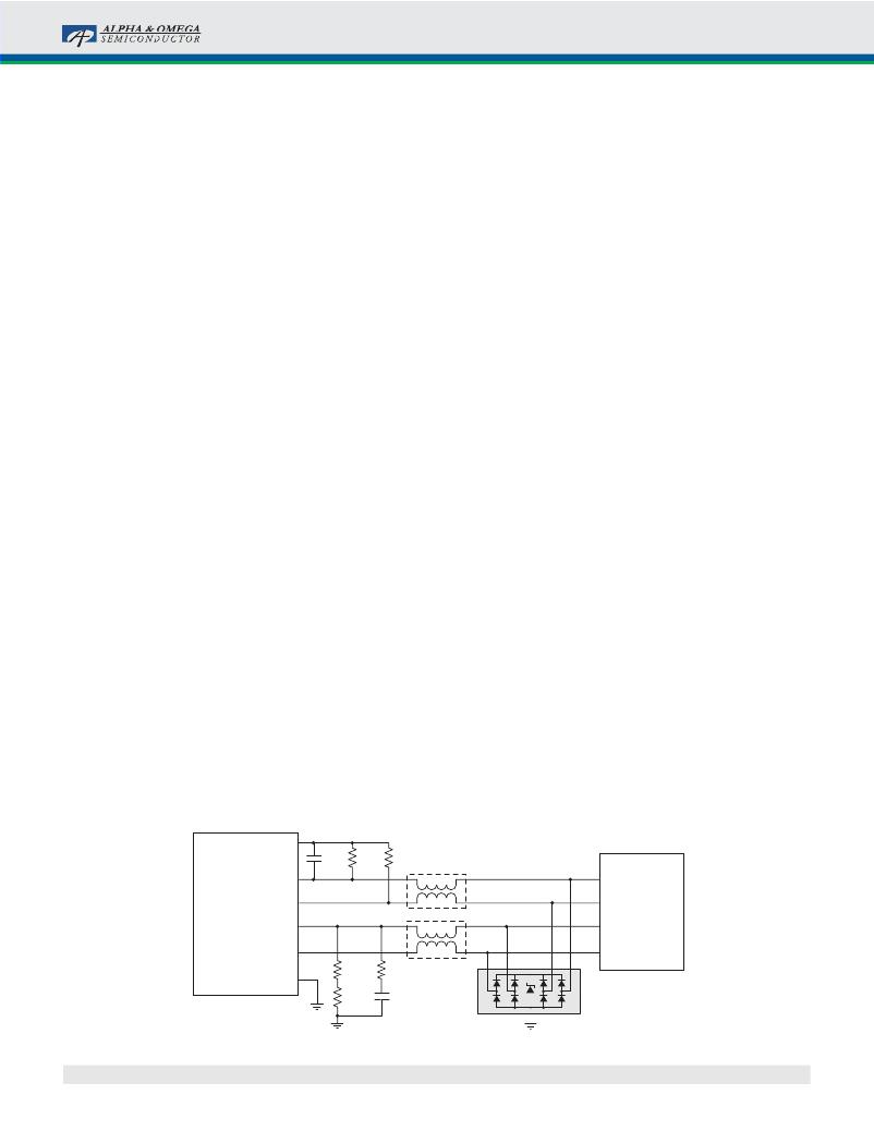
�TPAx+�
�IEEE� 1394�
�TPAx-�
�PHY�
�TPBx+�
�TPBx-�
�GND�
�1μF�
�56Ω�
�56Ω�
�56Ω�
�56Ω�
�IEEE� 1394�
�Connector�
�5.1k�
�270pF�
�AOZ8304A�
�IEEE1394� Port� Connection�
�Rev.� 1.1� August� 2011�
�www.aosmd.com�
�Page� 5� of� 8�
�发布紧急采购,3分钟左右您将得到回复。
相关PDF资料
AOZ8808DI-03
TVS DIODE ARRAY LOW CAP 10DFN
AOZ8808DI-05
TVS DIODE ARRAY LOW CAP 10DFN
AOZ8818DI-03
TVS DIODE ARRAY LOW CAP 10DFN
APA1FGRA04
SWITCH PUSH SPDT 0.05A 48V
APBE1FGRA04
SWITCH PUSH SPDT 0.05A 48V
APLVD400
VOLTMETER AC 3 1/2-DIGIT
APMR0016
MOD APMR 3-PH VAULT DET DIN RAIL
APS INT2012
INVERTER 2000W 230VAC OUT
相关代理商/技术参数
AOZ8304ADI-02
功能描述:TVS DIODE 3.3VWM 10VC 10DFN 制造商:alpha & omega semiconductor inc. 系列:- 包装:- 零件状态:上次购买时间 类型:转向装置(轨至轨) 单向通道:4 双向通道:- 电压 - 反向关态(典型值):3.3V(最大) 电压 - 击穿(最小值):3.5V 电压 - 箝位(最大值)@ Ipp:10V 电流 - 峰值脉冲(10/1000μs):25A(8/20μs) 功率 - 峰值脉冲:350W 电源线路保护:是 应用:以太网,电信 不同频率时的电容:5pF @ 1MHz 工作温度:-40°C ~ 85°C(TJ) 安装类型:- 封装/外壳:- 供应商器件封装:- 标准包装:3,000
AOZ8304DIL
功能描述:TVS DIODE 3.3VWM 10VC 10DFN 制造商:alpha & omega semiconductor inc. 系列:- 包装:带卷(TR) 零件状态:上次购买时间 类型:转向装置(轨至轨) 单向通道:4 双向通道:- 电压 - 反向关态(典型值):3.3V(最大) 电压 - 击穿(最小值):3.5V 电压 - 箝位(最大值)@ Ipp:10V 电流 - 峰值脉冲(10/1000μs):25A(8/20μs) 功率 - 峰值脉冲:350W 电源线路保护:是 应用:以太网,电信 不同频率时的电容:5pF @ 1MHz 工作温度:-40°C ~ 85°C(TJ) 安装类型:表面贴装 封装/外壳:10-UFDFN 裸露焊盘 供应商器件封装:10-DFN(2.6x2.6) 标准包装:3,000
AOZ8305DIL
制造商:AOS 功能描述:TVS
AOZ8308SO-02
功能描述:TVS DIODE 4CH HIGH SURGE SO-8 制造商:alpha & omega semiconductor inc. 系列:- 零件状态:在售 类型:齐纳 单向通道:2 电压 - 反向关态(典型值):2.3V (最大) 电压 - 击穿(最小值):2.8V 电压 - 箝位(最大值)@ Ipp:15V 电流 - 峰值脉冲(10/1000μs):25A(8/20μs) 功率 - 峰值脉冲:450W 电源线路保护:无 应用:通用 不同频率时的电容:1.5pF @ 1MHz 工作温度:-40°C ~ 125°C (TJ) 安装类型:表面贴装 封装/外壳:8-SOIC(0.154",3.90mm 宽) 供应商器件封装:8-SOIC 标准包装:3,000
AOZ8311DI-26
功能描述:TVS DIODE 26VWM 46VC DFN 制造商:alpha & omega semiconductor inc. 系列:- 包装:带卷(TR) 零件状态:有效 类型:齐纳 单向通道:1 双向通道:- 电压 - 反向关态(典型值):26V(最大) 电压 - 击穿(最小值):28.6V 电压 - 箝位(最大值)@ Ipp:46V 电流 - 峰值脉冲(10/1000μs):9A(8/20μs) 功率 - 峰值脉冲:410W 电源线路保护:无 应用:通用 不同频率时的电容:90pF @ 1MHz 工作温度:-40°C ~ 125°C (TJ) 安装类型:表面贴装 封装/外壳:2-UDFN 供应商器件封装:2-DFN (1.6x0.8) 标准包装:3,000
AOZ8312DI
功能描述:TVS DIODE 2.5VWM 9VC DFN 制造商:alpha & omega semiconductor inc. 系列:- 包装:带卷(TR) 零件状态:有效 类型:转向装置(轨至轨) 单向通道:- 双向通道:5 电压 - 反向关态(典型值):2.5V(最大) 电压 - 击穿(最小值):2.8V 电压 - 箝位(最大值)@ Ipp:9V 电流 - 峰值脉冲(10/1000μs):18A(8/20μs) 功率 - 峰值脉冲:160W 电源线路保护:是 应用:通用 不同频率时的电容:2.3pF @ 1MHz 工作温度:-40°C ~ 125°C (TJ) 安装类型:表面贴装 封装/外壳:12-UFDFN 裸露焊盘 供应商器件封装:12-DFN-EP(3.5x2.5) 标准包装:3,000
AOZ8318DI
功能描述:TVS DIODE 2.5VWM 5VC 10DFN 制造商:alpha & omega semiconductor inc. 系列:- 包装:剪切带(CT) 零件状态:有效 类型:转向装置(轨至轨) 单向通道:- 双向通道:4 电压 - 反向关态(典型值):2.5V(最大) 电压 - 击穿(最小值):2.8V 电压 - 箝位(最大值)@ Ipp:5V 电流 - 峰值脉冲(10/1000μs):25A(8/20μs) 功率 - 峰值脉冲:350W 电源线路保护:是 应用:以太网,电信 不同频率时的电容:3pF @ 1MHz 工作温度:-40°C ~ 125°C (TJ) 安装类型:表面贴装 封装/外壳:10-UFDFN 裸露焊盘 供应商器件封装:10-DFN(2.6x2.6) 标准包装:1
AOZ8328DI
功能描述:TVS DIODE 2.5VWM 16VC 10DFN 制造商:alpha & omega semiconductor inc. 系列:- 包装:带卷(TR) 零件状态:有效 类型:转向装置(轨至轨) 单向通道:- 双向通道:4 电压 - 反向关态(典型值):2.5V(最大) 电压 - 击穿(最小值):- 电压 - 箝位(最大值)@ Ipp:16V 电流 - 峰值脉冲(10/1000μs):25A(8/20μs) 功率 - 峰值脉冲:450W 电源线路保护:是 应用:以太网,电信 不同频率时的电容:2.8pF @ 1MHz 工作温度:-40°C ~ 85°C(TA) 安装类型:表面贴装 封装/外壳:10-UDFN 裸露焊盘 供应商器件封装:10-DFN(3x2) 标准包装:3,000